Super High Power Portable TV and FM Jammer Circuit Diagram
This is the Super High Power Portable TV and FM Jammer Circuit Diagram. There are still neighbors that keep annoying you by having loud the TV or the radio? Well I have you the solution. In fact all neighborhood will face your jamming waves at their TVs and radios, so be careful.
This Jammer is the improved version of the old `TV and FM jammer schematic` with the difference of much higher power. Many of you where asking for a stronger and wider effect but to be as portable as can be. Looking at the schematic you can see that, only the parts are changing keeping the basic circuit intact. Have in mind that this version needs heat sink and antenna to keep the transistor alive.
Super High Power Portable TV and FM Jammer Circuit Diagram

The power source comes from three 9 volt batteries in series, so we use 27 volts at input, and we get a power full 2,5 Watts at output.
You are going to need 70cm to 2 meter simple wire antenna.
As for the transistor Q its the 2N3553. Its a RF Power Silicon NPN Transistor in a TO39 type package designed to be used in amplifiers and oscillator applications in military and industrial equipment.
Usually found as an output driver, or in predriver stages in VHF equipment, but because here we dont care about the modulation of the signal but just the power, thats why we use it as a first and final output driver.
The transistor is specified at 175MHz and 28V to give: Output Power: 2.5W, Minimum Gain: 10dB and Efficiency: 50%.
The parts are: R1=10k, R2=2,2K, R3=100 C1=47uF/50V, C2=2.2nF, C3=10pF, SW=switch, B=Battery 9V.
The coil L should be closely wound 5 turns (start tunning with the closely wound distance of turns and then play with it and the C4 capacitor, to find the desired frequency )of enameled copper wire 1.5mm and internal coil diameter of 1cm (leads 2x20mm).
The variable capacitor C4 should be air trimmer capacitor rating 4 to 30 pf or the closest to this value.
Connect the batteries in series place the best heat sink for TO39 case you can get and pack it all in a small plastic box. Enjoy ;)
Datasheet file1: Click here to download 2n3553 datasheet.

Build a Positive And Negative Voltage Switching Supply
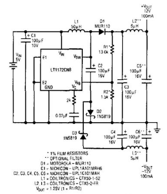
Build a Positive And Negative Voltage Switching Supply. An LT1172 generates positive and negative voltages from a 5-V input. The LT1172 is configured as a step-up converter. To generate the negative output, a charge pump is used. C2 is charged by the inductor when D2 is forward-biased and discharges into C4 when LT1172`s power switch pulls the positive side of C2 to ground.
Positive And Negative Voltage Switching Supply Circuit Diagram
Automotive LED Timing Light
A useful timing strobe can be constructed using high-brightness LEDs and a few common components. Ignition pulses from the number 1 cylinder high-tension lead are used to trigger the circuit via a home-made inductive pickup. Transistors Q1 & Q2 buffer and amplify the pulses from the pickup, which then drive the inputs of three Schmitt-trigger inverters (IC1a, IC1c & IC1f). Each positive pulse at the inverter inputs causes a low pulse at their outputs, forward-biasing D2 and immediately discharging the 6.8nF capacitor. When the capacitor is discharged, the inputs of the second bank of three inverters (IC1b, IC1d & IC1e) see a logic low level, so their outputs go high, driving Q3 into conduction and powering the LED array. After the pulse ends, the IC1a, IC1c & IC1f inverter outputs return high, reverse biasing D2.

However, it takes some time for the 6.8nF capacitor to charge to the logic high threshold voltage of the inverters’ inputs, effectively stretching the initial pulse width and lighting the LEDs for the required amount of time. The pickup can be salvaged from an old Xenon timing light or made up from a "C" type ferrite or powered iron core large enough to fit around a HT lead. Some experimentation will be required to determine the number of turns required to achieve reliable triggering. About 100 turns of light-gauge wire proved sufficient on the prototype. A cleat is used to close the magnetic path around the lead and is held in place with a large battery clip. Miniature screened microphone cable can be used to connect the pickup to the circuit, to prevent interference from other sources.
Read Full article[...]

However, it takes some time for the 6.8nF capacitor to charge to the logic high threshold voltage of the inverters’ inputs, effectively stretching the initial pulse width and lighting the LEDs for the required amount of time. The pickup can be salvaged from an old Xenon timing light or made up from a "C" type ferrite or powered iron core large enough to fit around a HT lead. Some experimentation will be required to determine the number of turns required to achieve reliable triggering. About 100 turns of light-gauge wire proved sufficient on the prototype. A cleat is used to close the magnetic path around the lead and is held in place with a large battery clip. Miniature screened microphone cable can be used to connect the pickup to the circuit, to prevent interference from other sources.
12 Volt Battery Guardian
Dont get caught with a flat battery; this easy-to-build circuit can cut off the power to a 12V fridge or car stereo system if the battery voltages drops below critical level. Electric fridges in vans and 4WDs are a great idea but if you are not careful, they can severely discharge the battery and leave you stranded. Maybe the battery will end up with severe damage as well. The same problem applies if you have a big stereo system and you like to play it without the motor running.

Main features:
- Cuts power to load (eg, fridge) when battery voltage drops below a preset level.
- 10A rating.
- Low power drain.
- Chirping sound during cut-out.
- Flashing LED indication during cut-out.
- Automatically reconnects power when battery recharged.
Operation on 12V is fine when the motor is running and battery charge is maintained but if the fridge is allowed to run for too long when the motor is stopped, it can flatten the battery in a relatively short time. This is where the Battery Guardian comes into play. It monitors the battery voltage and disconnects power to the fridge before the battery becomes too flat to allow the engine to be started again.
Parts layout:

PCB layout:

Circuit diagram:


Source: Silicon Chip 6 May 2002
1W BTL Audio Amplifier
The TDA8581(T) from Philips Semiconductors is a 1-watt Bridge Tied Load (BTL) audio power amplifier capable of delivering 1 watt output power into an 8-Wload at THD (total harmonic distortion) of 10% and using a 5V power supply. The schematic shown here combines the functional diagram of the TDA8551 with its typical application circuit. The gain of the amplifier can be set by the digital volume control input. At the highest volume setting, the gain is 20 dB. Using the MODE pin the device can be switched to one of three modes: standby (MODE level between Vp and Vp–0.5 V), muted (MODE level between 1 V and Vp–1.4 V) or normal (MODE level less than 0.5 V). The TDA8551 is protected by an internal thermal shutdown protection mechanism. The total voltage loss for both MOS transistors in the complementary output stage is less than 1 V.
Circuit diagram: Using a 5-V supply and an 8-W loudspeaker, an output power of 1 watt can be delivered. The volume control has an attenuation range of between 0 dB and 80 dB in 64 steps set by the 3-state level at the UP/DOWN pin: floating: volume remains unchanged; negative pulses: decrease volume; positive pulses: increase volume Each pulse at he Up/DOWN pin causes a change in gain of 80/64 = 1.25 dB (typical value). When the supply voltage is first connected, the attenuator is set to 40 dB (low volume), so the gain of the total amplifier is then –20 dB. Some positive pulses have to be applied to the UP/DOWN pin to achieve listening volume. The graph shows the THD as a function of output power. The maximum quiescent current consumption of the amplifier is specified at 10mA, to which should be added the current resulting from the output offset voltage divided by the load impedance.
Read Full article[...]
Circuit diagram:
 Using a 5-V supply and an 8-W loudspeaker, an output power of 1 watt can be delivered. The volume control has an attenuation range of between 0 dB and 80 dB in 64 steps set by the 3-state level at the UP/DOWN pin: floating: volume remains unchanged; negative pulses: decrease volume; positive pulses: increase volume Each pulse at he Up/DOWN pin causes a change in gain of 80/64 = 1.25 dB (typical value). When the supply voltage is first connected, the attenuator is set to 40 dB (low volume), so the gain of the total amplifier is then –20 dB. Some positive pulses have to be applied to the UP/DOWN pin to achieve listening volume. The graph shows the THD as a function of output power. The maximum quiescent current consumption of the amplifier is specified at 10mA, to which should be added the current resulting from the output offset voltage divided by the load impedance.
Safe Oscillator For Watch Crystals
This circuit was developed to allow watch crystals to be used in an existing CMOS oscillator circuit that was to run from a 12V supply. The problem is that these crystals only work up to a supply voltage of about 6V. Any more than that and the crystal will be over-driven, causing it to shatter. This circuit solves the problem by using LEDs 1 & 2 and a 470nF capacitor (C3) to limit the drive to the crystal to about 4V peak-to-peak. Note that it may be necessary to adjust C1 & C2 to ensure reliable start-up and stable oscillation with some crystals. However, the C1:C2 ratio should be maintained. As a bonus, the two LEDs both glow, giving a visual indication that the oscillator is working.

Editors note:
The relatively high values used here for capacitors C1 & C2 will load the crystal, which means that the oscillator will run at less than the nominal crystal frequency (32.768kHz).
Read Full article[...]

Editors note:
The relatively high values used here for capacitors C1 & C2 will load the crystal, which means that the oscillator will run at less than the nominal crystal frequency (32.768kHz).
Battery Charging Indicator For Mains Adaptor
Although you may well be the proud owner of the very latest NiCd battery charger, you may still come across the odd incompatible battery, for example, one having a rare voltage or requiring a much higher charging current than can be supplied by your off-the-shelf charger. In these cases, many of you will resort to an adjustable mains adaptor (say, a 500-mA type) because that is probably the cheapest way of providing the direct voltage required to charge the battery. Not fast and not very efficient, this rustic charging system works, although subject to the following restrictions:

Read Full article[...]

- You should have some idea of the charging current. In case you use an adaptor which is adjustable but of the unregulated, low output current type, you can adjust the current by adjusting the output voltage.
- You have to know if the current actually flows through the battery. A current-detecting indicator is therefore much to be preferred over a voltage indicator.
- To prevent you from forgetting all about the charging cycle, the indicator should be visible from wherever you pass by frequently. Using the circuit shown here, the LED lights when the baseemitter potential of the transistor exceeds about 0.2 V. Using a resistor of 1 ? as suggested this happens at a current of about 200 mA, or about 40 mA if R1 is changed to 4.7?. The voltage drop caused by this indicator can never exceed the base-emitter voltage (UBE) of the transistor, or about 0.7V. Even if the current through R1 continues to increase beyond the level at which UBE = 0.7 V, the base of the transistor will absorb the excess current. The TO-220 style BU406 transistor suggested here is capable of accepting base currents up to 4A. Using this charging indicator you have overcome the restrictions 2 and 3 mentioned above.
Subscribe to:
Posts (Atom)