Luggage Security System

While traveling by a train or bus, we generally lock our luggage using a chain-and-lock arrangement. But, still we are under tension, apprehending that somebody may cut the chain and steal our luggage. Here is a simple circuit to alarm you when somebody tries to cut the chain. Transistor T1 enables supply to the sound generator chip when the base current starts flowing through t. When the wire (thin enameled copper wire of 30 to 40 SWG, used or winding transformers) loop around the chain is broken by somebody, the base of transistor T1, which was earlier tied to positive rail, gets opened. As a result, transistor T1 gets forward biased to extend the positive supply to the alarm circuit. In idle mode, the power consumption of the circuit is minimum and thus it can be used for hundreds of travel hours. To enable generation of different alarm sounds, connections to pin 1 and 6 may be made as per the table.

Luggage Security System Circuit Diagram
Read Full article[...]

Two Basic Motor Speed Controllers

Here are two simple 12V DC motor speed controllers that can be built for just a few dollars. They exploit the fact that the rotational speed of a DC motor is directly proportional to the mean value of its supply voltage. The first circuit shows how variable voltage speed control can be obtained via a potentiometer (VR1) and compound emitter follower (Q1 & Q2). With this arrangement, the motor’s DC voltage can be varied from 0V to about 12V. This type of circuit gives good speed control and self-regulation at medium to high speeds but very poor low-speed control and slow starts. The second circuit uses a switchmode technique to vary motor speed.

Two basic motor speed controllers circuit schematic
Fig.1: a very simple motor speed controller based on a compound emitter follower (Q1 & Q2).

Here a quad NOR gate (IC1) acts as a 50Hz astable multivibrator that generates a rectangular output. The mark-space ratio of the rectangular waveform is fully variable from 20:1 to 1:20 via potentiometer VR1. The output from the multivibrator drives the base of Q1, which in turn drives Q2 and the motor. The motor’s mean supply voltage (integrated over a 50Hz period) is thus fully variable with VR1 but is applied in the form of high-energy "pulses" with peak values of about 12V.

Two basic motor speed controllers circuit schematic
Fig.2: this slightly more complicated circuit gives better low speed control and higher torque.

This type of circuit gives excellent full-range speed control and gives high motor torque, even at very low speeds. Its degree of speed self-regulation is proportional to the mean value of the applied voltage. Note that for most applications, the power transistor (Q2) in both circuits will need to be mounted on an appropriate heatsink.
Read Full article[...]

Alarm Clock With Day Selector

This  circuit disables an alarm clock on Saturdays and Sundays when people like to sleep in but enables normal operation on Mondays to Fridays so that people rise in time for work or school. The core of the circuit is a 4017 decade counter which acts as the day counter and it is used in conjunction with a desk clock which acts the alarm and a watch module with alarm function which provides one clock pulse very day to the 4017. In operation, the watch module feeds a day pulse via transistor Q3 to the clock input of IC1. This has seven outputs connected via day switches (S1-S7) and diodes D3-D9 to Q1 which disables the alarm signal to the speaker via transistor Q2. LEDs1-7 indicate the actual day (if you forget!).

Circuit diagram:

Alarm-clock-with-day Selector Circuit Diagram

Alarm Clock With Day Selector Circuit Diagram

To set the system, set the desk clock for the correct time and for the desired alarm time (eg, 6’o’clock). The watch module is set to the correct time and its alarm set to midnight. The day counter, IC1, is set to the correct day, as indicated by the LEDs, by pushing switch S12 and closing switch S8 or S9. S8 is normally left open to conserve the battery by leaving the LEDs off. As shown on the circuit, switches S1-S7 are set to sound the alarm on Mondays to Fridays and disable it on Saturday and Sunday. However, you can change the days to suit your work habits.

Author: Rasim Kucalovic - Copyright: Silicon Chip Electronics

Read Full article[...]

Park Aid Modification Circuit

Three-step beeps signal bumper-barrier distance, Infra-red operation, indoor use

This modification was designed on request: some people prefer an audible alert instead of looking at the LED display, making easier the parking operation. The original Park-aid circuit was retained, but please note that the input pins of IC2B, IC2C and IC2D are reversed. LEDs D5, D6 and D7, as also resistors R12, R13 and R14 are omitted. IC2B, IC2C and IC2D outputs drive resistors R15, R16 and R17 through D8, D9 and D10 respectively, in order to change the time constant of a low frequency oscillator based on the 555 timer IC4. This allows the Piezo sounder to start beeping at about 2 times per second when bumper-wall distance is about 20 cm., then to increase the beeps to about 3 per second when bumper-wall distance is about 10 cm. and finally to increase further the beeps frequency to more than 4 beeps per second when the distance is about 6 cm. or less.

Circuit diagram:

Park-Aid Modification Circuit Diagram

Park-Aid Modification Circuit Diagram

Parts:

R15_____________3K3 1/4W Resistor
R16___________330K 1/4W Resistor
R17___________470K 1/4W Resistor
R18___________150K 1/4W Resistor
C6______________1µF 63V Electrolytic or Polyester Capacitor
D8,D9,D10____1N4148 75V 150mA Diodes
IC4_____________555 Timer IC
BZ1___________Piezo sounder (incorporating 3KHz oscillator)

Source : www.redcircuits.com

Read Full article[...]

555 Timer With Variable On Off Times

This circuit enables the on/off times of a 555 timer to be independently varied over a wide range. This is not possible with a conventional 555 circuit with the RC network being charged from the positive supply rail and discharged via pin 7. Instead, the capacitor at pins 2 & 6 of IC1 is charged and discharged from the output at pin 3. Furthermore, the charging and discharging circuits are different, being isolated by diodes D1 & D2.

555 Timer Circuit With Variable On/Off Times circuit schematic

Therefore the capacitor at pins 2 & 6 is charged via diode D2 and trimpot VR2 and discharged via D1 and trimpot VR1. With this arrangement you can have very long on times combined with very short off times and vice versa, or you can adjust the duty cycle to exactly 50% and so on. This circuit also employs a second 555 timer (IC2) as an inverter so that complementary pulses are available, if required. If not, delete IC2.
Read Full article[...]

Fuse Box BMW R1150RT 2002 Diagram

Fuse Box BMW R1150RT 2002 Diagram - Here are new post for Fuse Box BMW R1150RT 2002 Diagram.

Fuse Box BMW R1150RT 2002 Diagram


Fuse Box BMW R1150RT 2002 Diagram

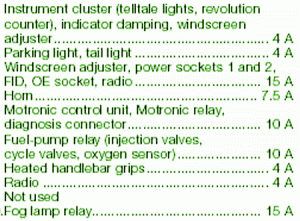
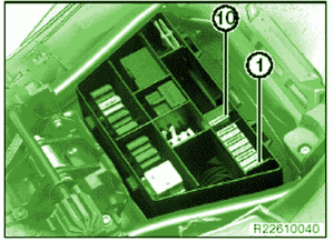
Fuse Panel Layout Diagram Parts: instrument cluster, telltale light, revolution counter, indicator clamping, windscreen adjuster, parking light, tail light, windscreen adjuster, power socket, radio, horn, motronic control unit, motronic relay, diagnosis connector, fuel pump relay, oxygen sensor, heated handlebar grips, radio, fog lamp relay.
Read Full article[...]

Build a 16 LED Chaser Circuit Diagram

This 16 LED Chaser Circuit Diagram is a double direction flash. Similar to Digital Ping- Pong 1, there is a movement of a lit dot, up and down along the LEDs length.

16 LED Chaser Circuit Diagram

16 LED Chaser Circuit Diagram


When the D16 lit the situation changes and there is a reverse movement. Lit D15-14 ……D16, is lit making circles when the circuit is under power. The IC1 is an unstable flip- flop supplying with stable frequency pulses (the frequency can be changed by TR1, adjusting the velocity of the LEDs up and down).

This frequency supplies the IC3 (which is a 4-Bit UP and DOWN counter) through 2 gates A-B of the IC2. The output counter supplies the IC4 that is the driver of the LEDs. The parts C- D of The IC2, make a R-S flip- flop, that changes situation, when the edge LEDs D1 and D16 lit.

We have an electronic limit for the situation change. In proportion the shape we make with the LEDs, we can have the proportionate optional result, making various effects.

Part List

R1= 100Kohms
R2= 220Kohms
R3= 470 ohms
TR1= 1Mohms
C1= 330nF 100V MKT
D1-16= LED 5mm
IC1= 555
IC2= 7400
IC3= 74193
IC4= 74154
Read Full article[...]

3 Transistor Audio Amplifier Circuit

Description
Here is a little audio amplifier similar to what you might find in a small transistor radio. The input stage is biased so that the supply voltage is divided equally across the two complimentary output transistors which are slightly biased in conduction by the diodes between the bases. A 3.3 ohm resistor is used in series with the emitters of the output transistors to stabilize the bias current so it doesnt change much with temperature or with different transistors and diodes. As the bias current increases, the voltage between the emitter and base decreases, thus reducing the conduction.
Input impedance is about 500 ohms and voltage gain is about 5 with an 8 ohm speaker attached. The voltage swing on the speaker is about 2 volts without distorting and power output is in the 50 milliwatt range. A higher supply voltage and the addition of heat sinks to the output transistors would provide more power. Circuit draws about 30 milliamps from a 9 volt supply. 
Read Full article[...]

Mobile Cellphone Battery Charger Circuit

Charging of the mobile phone, cellphone battery is a big problem while traveling as power supply source is not generally accessible. If you keep your cellphone switched on continuously, its battery will go flat within five to six hours, making the cellphone useless.

A fully charged battery becomes necessary especially when your distance from the nearest relay station increases. Here’s a simple charger that replenishes the cellphone battery within two to three hours. Basically, the charger is a current-limited voltage source. Generally, cellphone battery packs require 3.6-6V DC and 180-200mA current for charging. These usually contain three NiCd cells, each having 1.2V rating.

Current of 100mA is sufficient for charging the cellphone battery at a slow rate. A 12V battery containing eight pen cells gives sufficient current (1.8A) to charge the battery connected across the output terminals. The circuit also monitors the voltage level of the battery. It automatically cuts off the charging process when its output terminal voltage increases above the predetermined voltage level.
Circuit Diagram:
Parts
  • P1 = 20K
  • P2 = 20K
  • R1 = 390R
  • R2 = 680R
  • R3 = 39R-1W
  • R4 = 27K
  • R5 = 47K
  • R6 = 3.3K
  • R7 = 100R-1W
  • C1 = 4.7uF-25V
  • C2 = 0.01uF
  • C3 = 0.001uF
  • D1 = 5.6V-1W Zener
  • D2 = 3mm. Red LED
  • Q1 = SL100
  • S1 = On/Off Switch
  • B1 = 1.5vx8 AA Cells in Series
  • IC1 = NE555 Timer IC 
Circuit Operation
Timer IC NE555 is used to charge and monitor the voltage level in the battery. Control voltage pin 5 of IC1 is provided with a reference voltage of 5.6V by zener diode D1. Threshold pin 6 is supplied with a voltage set by P1 and trigger pin 2 is supplied with a voltage set by P2. When the discharged cellphone battery is connected to the circuit, the voltage given to trigger pin 2 of IC1 is below 1/3Vcc and hence the flip-flop in the IC is switched on to take output pin 3 high. When the battery is fully charged, the output terminal voltage increases the voltage at pin 2 of IC1 above the trigger point threshold.
This switches off the flip-flop and the output goes low to terminate the charging process. Threshold pin 6 of IC1 is referenced at 2/3Vcc set by P1. Transistor Q1 is used to enhance the charging current. Value of R3 is critical in providing the required current for charging. With the given value of 39-ohm the charging current is around 180 mA. The circuit can be constructed on a small general-purpose PCB.
For calibration of cut-off voltage level, use a variable DC power source. Connect the output terminals of the circuit to the variable power supply set at 7V. Adjust P1 in the middle position and slowly adjust P2 until LED (D2) goes off, indicating low output. LED should turn on when the voltage of the variable power supply reduces below 5V. Enclose the circuit in a small plastic case and use suitable connector for connecting to the cellphone battery.
Read Full article[...]